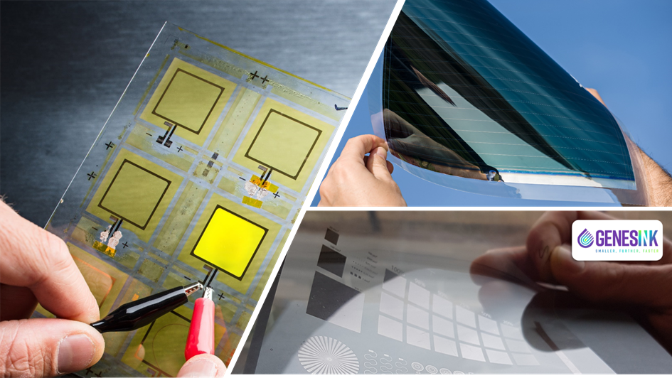
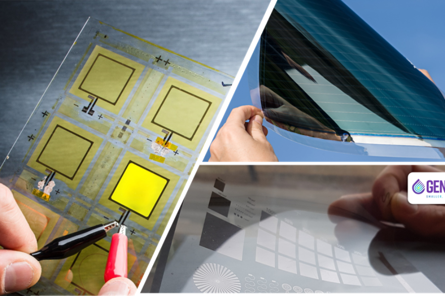
GenesInk develops conductive and semi-conductive inks to enable new functionalities such as transparency, flexibility, and stretchability for the consumer electronics market. What makes GenesInk unique is its capability to solve technological issues such as reduce form factor, increase the tracks finesse and electrical performance resulting in highly functional, lightweight, and aesthetic electronic devices.
GenesInk is looking to integrate new European consortia to implement its nanoinks into energy generation and storage applications. we propose to offer our know-how and expertise in the conception of main nanomaterials for the different layers in PV (HTL, ETL, transparent electrode and top electrode). GenesInk is also aiming to develop new Ag nanoinks compatible with silicon-based photovoltaics.
If our expertise is of interest for you and you have a project idea in mind do not hesitate to contact our R&I team with high expertise in European proposals preparation and projects management: vanessa.douet@genesink.com; benjamin.dhuiege@genesink.com ; rita.faddoul@genesink.com.


