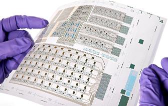
Printed transistors scale up to system prototypes
The first proofs of concept allowing the realization of subsystems manufactured by printing have just been realized with a second generation transistor technology. This step paves the way for the development of application demonstrators with optimized electronic integration.
Developed for more than 10 years at the Liten, an institute of CEA Tech, printed electronics on flexible organic media has taken an important step forward in the European ATLASS project. While proof of concept had already been done on the scale of components and simple circuits, the printing of transistors on plastic substrates had not yet been demonstrated on a pilot line with sufficient performance and efficiency levels for the manufacture of complex circuits and subsystems. It is now done!
Working closely with ink and printing equipment suppliers, Liten has optimized the materials and printing process (including engraving of printing rollers) to achieve the efficiencies required to scale up. The process reliability has also been improved to achieve a near-zero defect rate and perfect reproducibility of the components. Several samples of a few hundred to a few thousand transistors were produced with 0 defects (100% functional components). This optimization and maturation work has enabled the prototyping and realization of functional demonstrators based on printed transistor circuits in the field of the Internet of Things and Intelligent Sensor Surfaces. The interest of the technology will now be tested for various applications.


