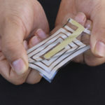
The development of IoT, sensors and smaller electronic devices pushes printed electronic manufacturing towards its limit. Form factor reduction is a must, and screen-printed electronics require now finer printed lines as well as thinner substrates.
When targeting fine lines, current products show their limits: strong resistivity, poor homogeneity, step effect for multilayer printing.
When looking to decrease the device thickness, substrate choice is a key parameter. Reduction of substrate thickness below 50µm, down to thickness such as 25µm, allows new applications. It is today limited by substrate surface waves resulting from adhesion during curing, but also by material thickness and dielectric passes.
GenesInk team will expose the possibilities for fine line printing as well as ultra-thin substrate electronics thru examples and existing technical solutions available at mass production scale.
Schedule (click on selected date and time to register):
- September 26th, 2019.
- Duration: 20 – 30 min
Contact information :
Grégoire STAELENS
Email: gregoire.staelens@genesink.com
Phone: +33 4 42 37 05 84


